Blockset described on this wiki is deprecated since 2012.
For Model Based Design (MBD), use the free MPLAB Device Blocks for Simulink, tool from Microchip.
Updated Rapid Control Prototyping (RCP) custom projects are published at: https://lubin.kerhuel.eu.
SPI communication between two dsPIC
Contents
Description
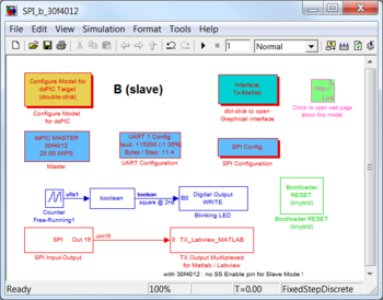
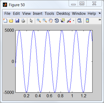
In this example, a variable is transmitted from one microcontroller (noted A) to another (noted B) through a SPI bus. A 4Hz Sinus is generated in the (A) and sent every 1ms to the microcontroller (B) through a SPI BUS. Then, (B) send the received value to the PC through its UART peripheral. The Matlab rs232gui interface plot the received values.
Characteristics of SPI transmissions
SPI acronym stands for Serial Peripheral Interface. It is a numerical bus that in its standard form use 4 wires :
- One clock (clk) *One output data (SDO for Serial Data Out) *One input data (SDI for Serial Data In) *One Chip Select (CS)
This type of bus can connect one master to one or many slave. The three first wires clk, SDO and SDI are connected to all slave peripheral. However, each slave will have its Chip Select (CS) pin connected to a different digital output pin of the master. The Chip Select pin on the slave peripheral is for the SPI peripheral (I do not mean this is the Chip Select of the slave if it has one). The Chip Select pin of the master could be any pin. The Chip Select input signal activates the SPI peripheral of the slave.
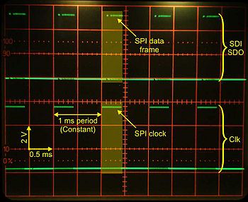
The bus is clocked. The clock is driven by the master. The clock frequency must be less or equal than the max acceptable frequency for the slave. In this example, we clocked it at 39kHz which make it a slow bus. This clock is activated only during transmission. Thus the master stops the clock when no slaves are selected.
ASlave can transmit a data only if it is selected by the master. The SDI and SDOdata wires provide a full duplex bus: the slave can send a data while the mastersend it a data.
The SPI bus presentation is beyond the scope of this example. Readers are referred to the Wikimedia page on the SPI bus for further information.
Three blocks related to the SPI bus are available in the dsPIC blockset library.
The SPI Configuration configure SPI peripheral and some bus characteristics like the active state of both clock and data (defining the so called bus mode), the bus frequency. This block is required as soon as one SPI peripheral is used.
The block SPI_Input_Output allow to read/write data on the SPI bus. Many copy of this block could be present in the simulink model so as to read/Write several data from/to the bus.
The block SPI_Input_Output_Interrupt_Driven is an interrupt driven version which will be able to read/write in background data to/from the SPI bus.
Electronics
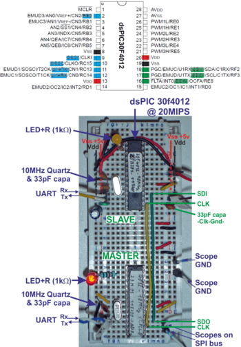
We use the same prototyping board described in the PWM example. And a bootloader capable of flashing the binary into the chip through UART is also used as it is described here.
The PWM wire is removed.
Data are sent from A ==> B but no data are sent from B ==> A. Thus only one data wire is required here. The SS pin (that is the SPI chip select when configured as slave) is not workable on the dsPIC 30f4012. The SPI slave peripheral is always enabled. Thus, the CS wire is not required also. Thus only two wires are necessary : The Clk for the Clock. The SDO (output) pin of A is connected to the SDI (input) of B. .
Simulink models
Two simulink models generate the code for the dsPIC (A) and the dsPIC (B). The common part of theses two model has been descriped on the PWM example.
Let’s considere only the specific parts related to the SPI bus of these two models.
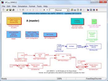
Model A: Emission
The model A creates an internal sine wave signal of type int16 with amplitude 5000 and frequency 4 Hz. The sine wave generated values are transmitted to microcontroller (B) (corresponding to model B) through SPI…
Optimized method for sine wave generation was described in the PWM example.
Execution time use 2.25% of a time step.
